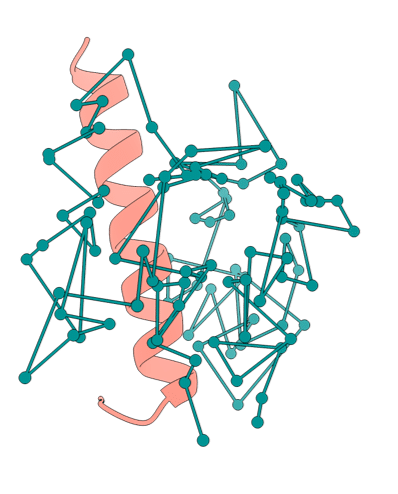
By combining biotechnology, nanotechnology, and data science, PUXANO offers a proprietary technology platform designed to accelerate structure-based protein research, from sequence to structure. Our technologies address key bottlenecks in the standard structural biology pipeline, including construct design, protein expression, purification, and high-resolution structure determination. The innovative nature of our platform is evidenced by the numerous competitive regional and international research grants awarded to PUXANO since its inception.

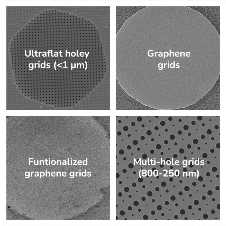
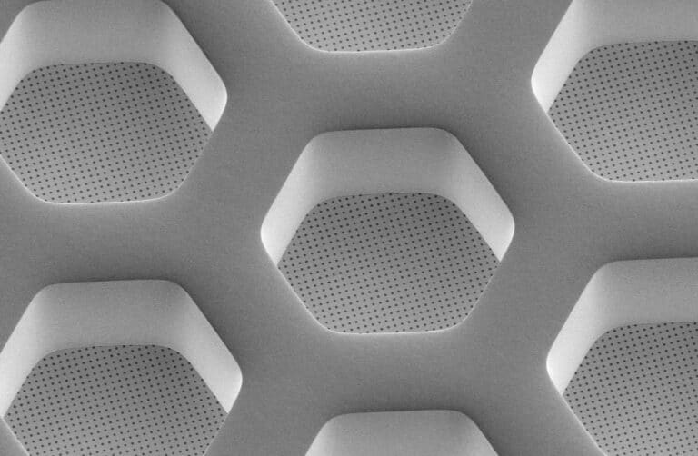
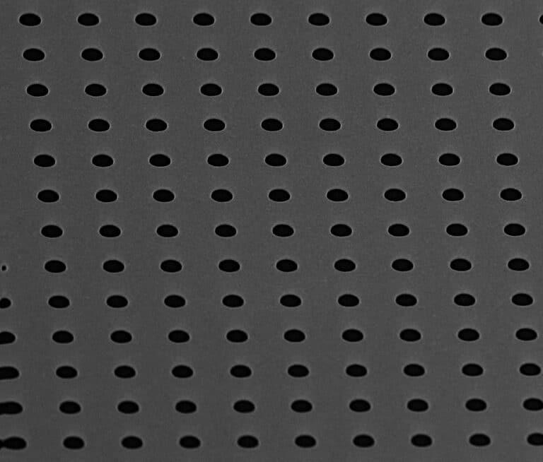
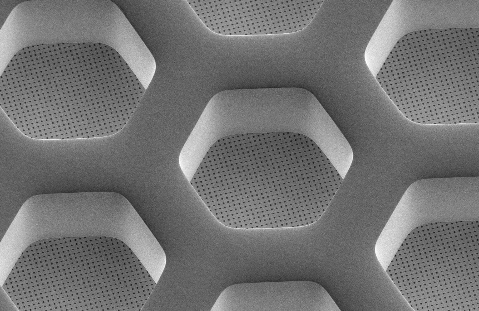
PXN Grids are advanced, customizable electron microscopy grids designed for high-throughput cryo-EM sample screening. Developed by our expert nanoengineering team in a dedicated cleanroom, these grids are fabricated using semiconductor-grade techniques. We offer full customization of grid design, material, and composition, tailoring each grid to meet specific research needs. Options include square or hexagonal mesh frameworks in varying sizes, thin films (metallic or carbon) with holey patterns ranging from 2000 µm to 250 nm, and film thicknesses between 30 and 100 nm. Additionally, we can deposit continuous thin films, such as graphene, which can be functionalized to create affinity grids.
Our proprietary grid portfolio is designed to overcome key challenges in cryo-EM, such as preferred particle orientation, uneven particle distribution, low protein yield, and suboptimal ice thickness. In addition to ultraflat holey cryo-EM and high-quality graphene grids, we have developed different speciality grids including Multi-hole grids with varying hole sizes, nanoparticle-specific cryo-EM grids, Tilted grids and Affinity grids functionalized with VHHs. These advanced grids, in combination with tailored grid priming techniques and customized image processing protocols, offer greater control over sample preparation and significantly enhance the success of cryo-EM projects.
